Packaging
Assembling microtechnical elements into a product for the macro world
Various microtechnologically manufactured elements need to be integrated and protected from interfering influences. At the same various physical interfaces are realized to connect the outside.
Chip-level packaging
Micro-Chips are connected to the substrate and protected
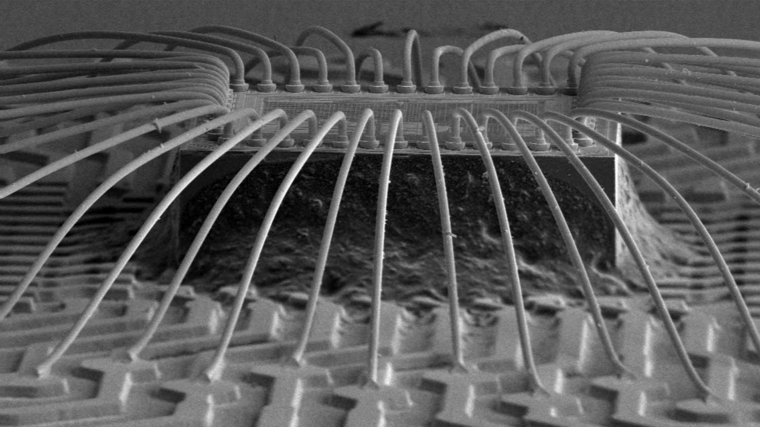
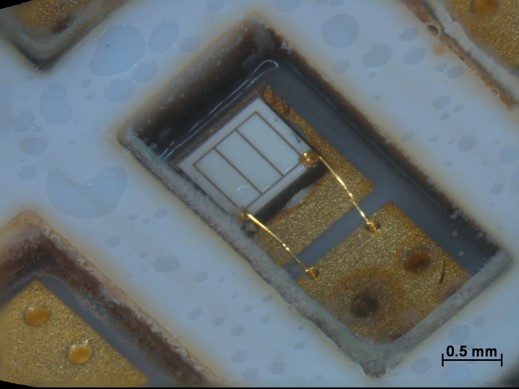
Electrical connections from the micro-chip to the substrate are enabled by wire-bonding or die-bonding technologies. Hermetical sealing, heat dissipation, mechanical integrity, as well as optical and fluidic interfaces, are highly customizable aspects.

Wafer-level packaging
Arrays of micro-elements are joined together to a product in a single process step
Complex systems often require that arrays of individual elements are manufactured on different substrate technologies and subsequently joined together. Joining techniques such as soldering (eutectic, thermocompression) and bonding (anodic, fusion, polymer layer) are thereby applied and optimized according to customer requirements.

Miniaturized, heterogeneous system
Novel solution are often realized by combining different technologies in a product
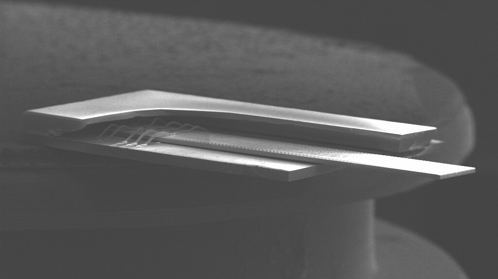
Micro-elements, based on different technologies, are joined together to form a miniaturized system. The advantages of the individual techniques are combined and novel solutions are realized.

Prof. Dr. Tobias Lamprecht
IMP Institut für Mikrotechnik und Photonik Institutsleiter IMP; Professor für Mikrotechnik
+41 58 257 34 22 tobias.lamprecht@ost.ch

Dietmar Bertsch
IMP Institut für Mikrotechnik und Photonik Senior Research Engineer, Fachverantwortlicher Packaging
+41 58 257 34 71 dietmar.bertsch@ost.ch


