Micro- and Nanostructures
The core of microtechnology
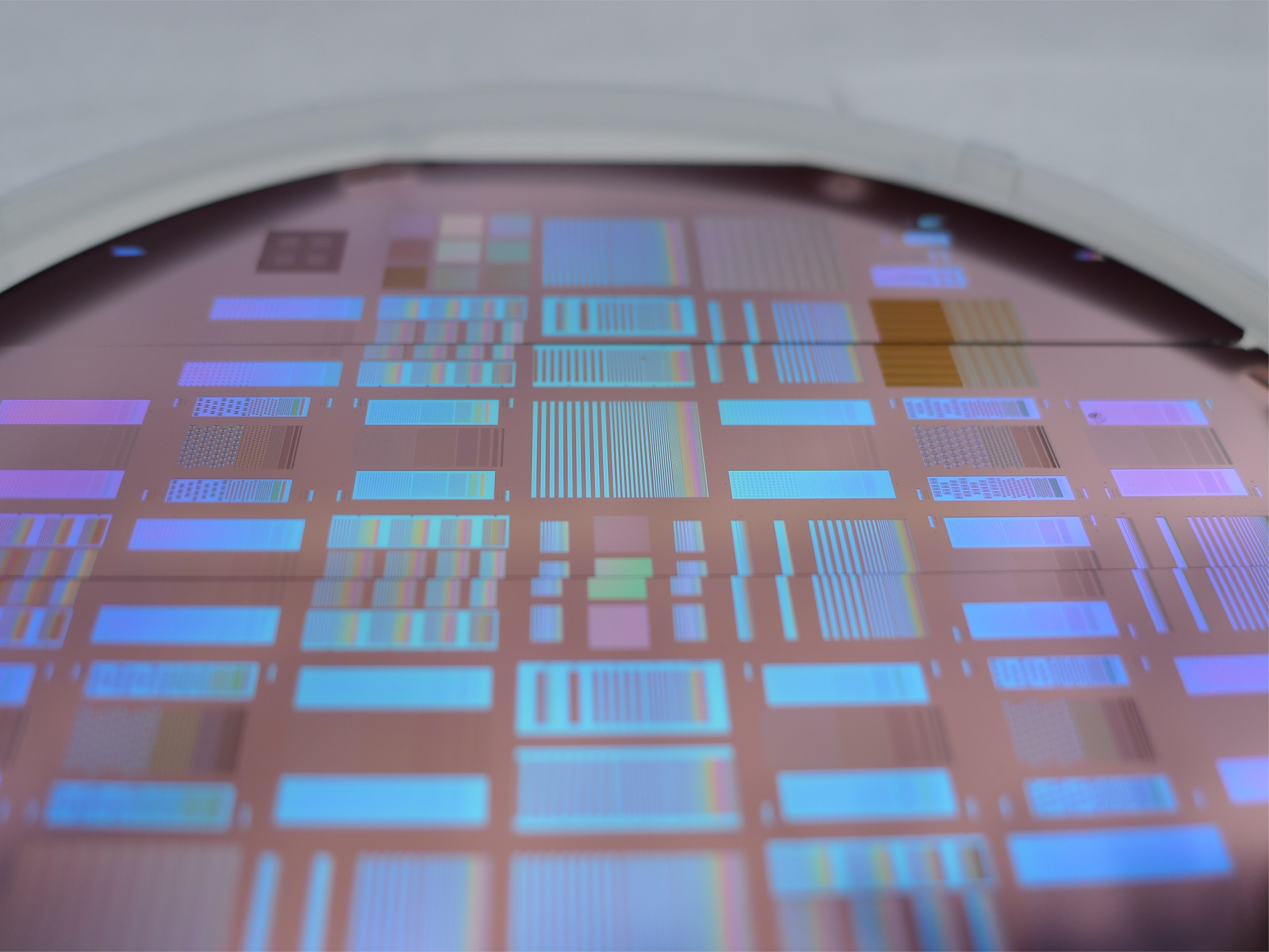
Ultra-small structures in the scale of micro- and nanometers are used in various applications, e.g. sensor technology. For this purpose, a resist is structured using lithographic methods, such as photolithography. These structures are being transferred into metallic or dielectric thin films by wet or dry etching (surface micromachining). Alternatively, the structures can be etched into substrates such as silicon or glass (bulk micromachining).
Lithography: structures in resist
Lithographic methods were originally developed for the fabrication of integrated microelectronic circuits. But over time lithography has become a basic process for microfabrication. The required accuracy, process time and efficiency play an important role when chosing the right lithographic method.
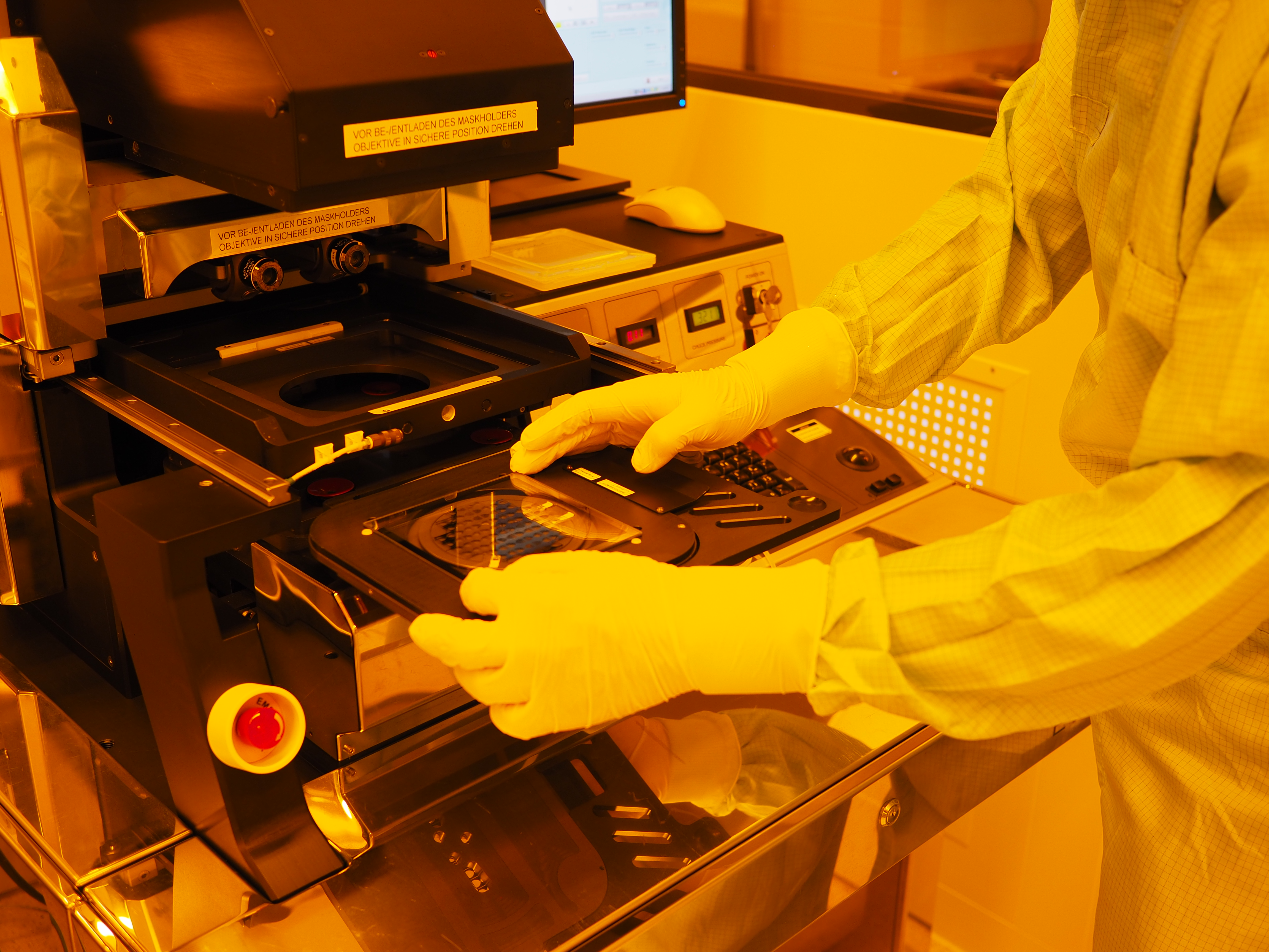
From process design and optimization to production and industry transfer, we offer the following services:
- Mask design and coordianation of fabrication
- Spin coating, spray coating, lamination
- Photolithographie, UV-NIL, microcontact printing
- Fabrication of multilayer structures
- Design qualification of precesses and tools
- Implementation and commissioning of processes at customers own sites
Typical applications are:
- Masking for dry and wet etching (e.g. DRIE, BHF)
- Patterning of thin films (e.g. lift-off)
- Patterning in preparation for electroplating (e.g. UV-LIGA)
- Direct fabrication of micro structured components (e.g. SU-8)
Wet chemical etching
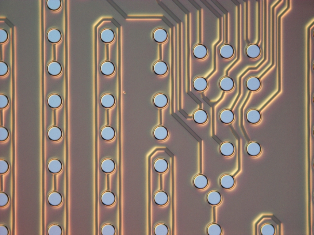
The aim of wet chemical etching is the straightforward, cost effective fabrication of microstructures. For this purpose, the previously masked substrates are dipped into an etch bath or sprayed with the etchant. In general, wet chemical etching features a high selectivity, low contamination and surface damage, a high degree of uniformity and reproducibility as well as a well controlled ethc rate. In addition only relativley simple and inexpensive infrastructure is needed and several substrates can be processes in parallel.
- Wet chemical cleaning of substrates (silicon, borofloat, quartz,...)
- Anisotropic etching of silicon
- Patterning of metals (Al, Au, Ag, Cr, Cu, Ti, W/Ti, Ni, ...)
- Paterning of various glasses
- Use of standardized etchants or specific etchant development
Dry etching
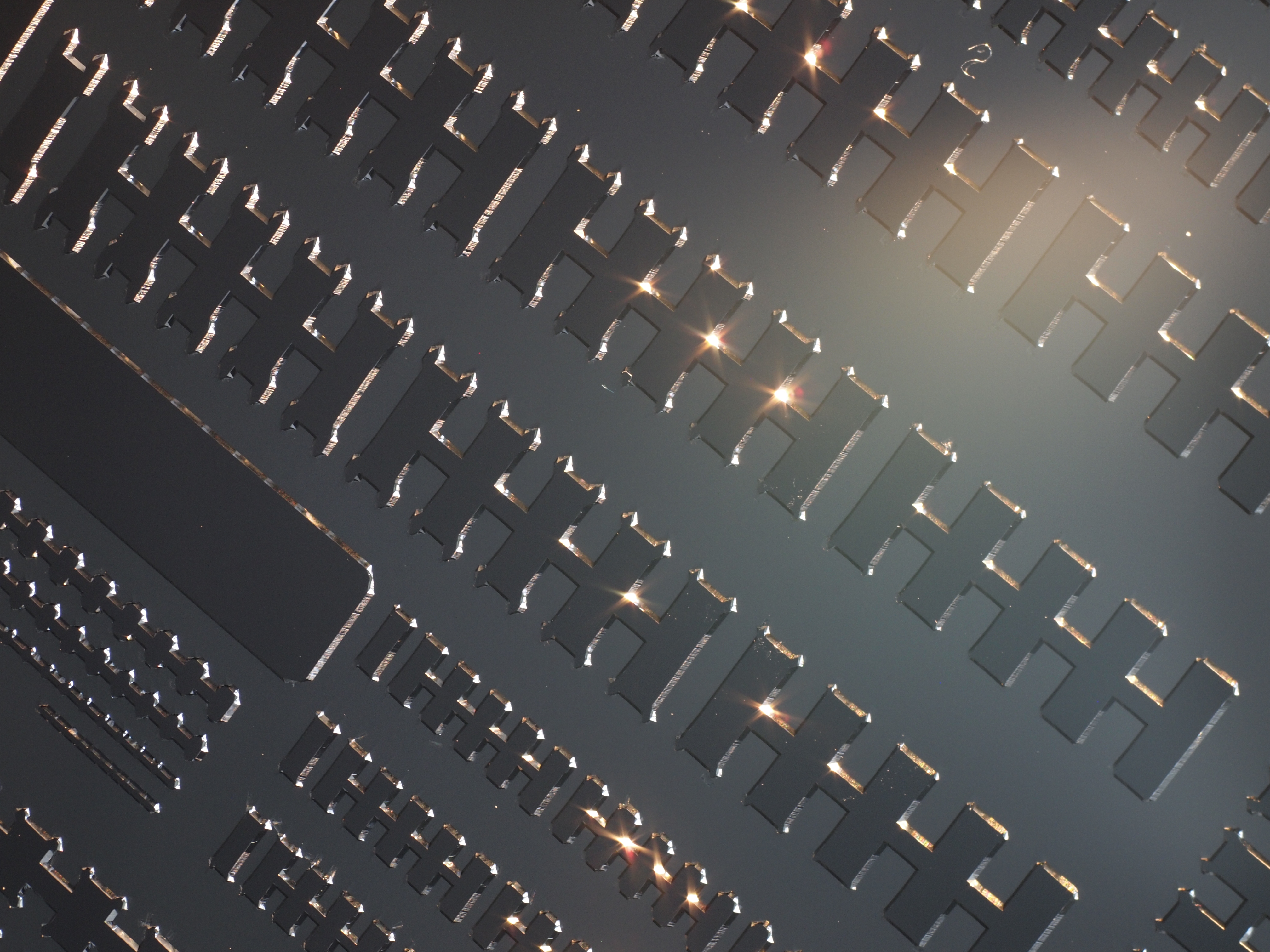
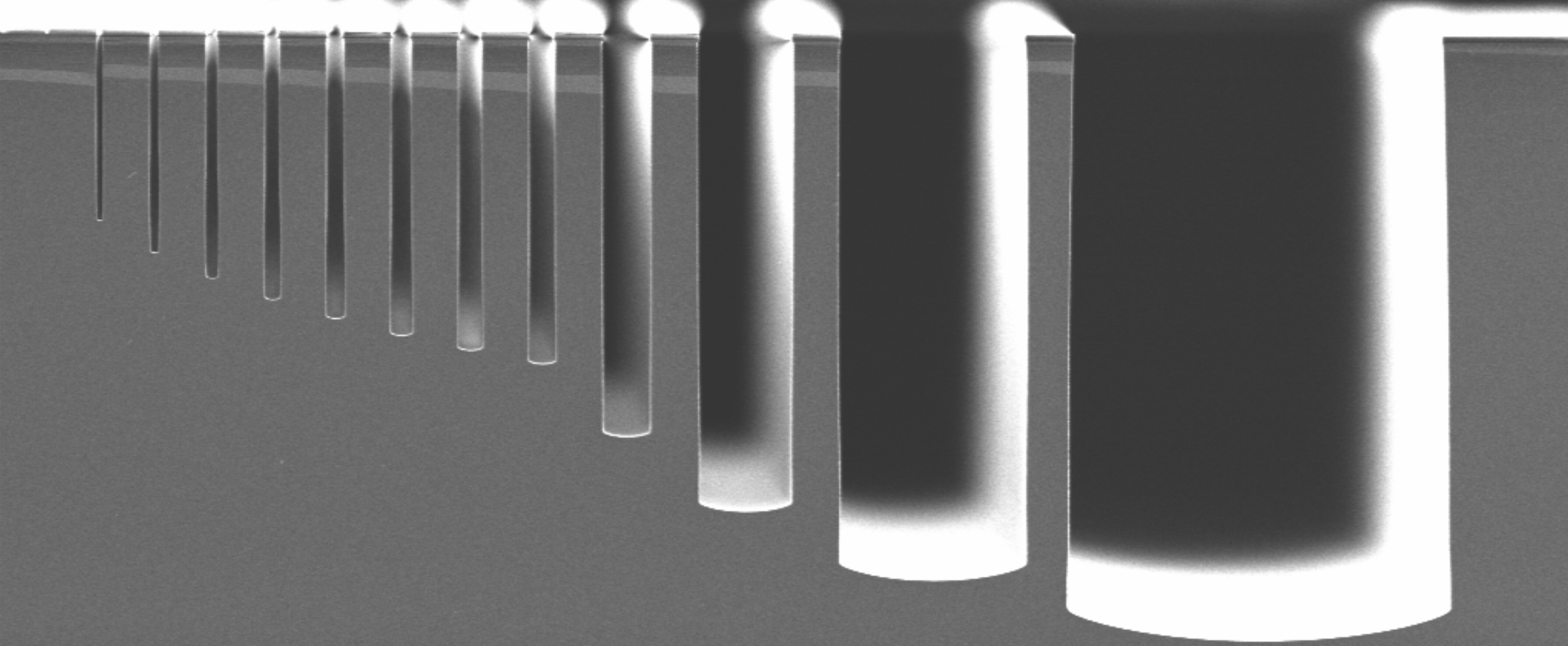
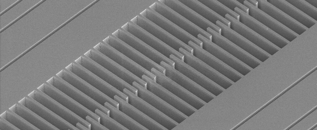
The aim of dry etching process is the fabrication of high resolution, complex microstructures. To do so, the substrates are exposed to a plasma. Physical dry etching occurs solely as a result of material removal through the impact of accelerated particles (ions, electrons or photons), while chemical dry etching processes rely on a chemical reaction mechanism. The combination of both processes is of high interest for the fabrication of integrated circuits an micromechanical components. These processes enable us to produce very small structures with high aspect ratios.
Das Ziel trockenchemischer Ätzprozesse ist die Herstellung komplexer, hochaufgelöster Mikrostrukturen. Dazu werden die Substrte einem Plasma ausgesetzt. Beim physikalischen Trockenätzen erfolgt der Materialabtrag allein durch den Beschuss der Oberfläche mit Ionen, während beim chemischen Trockenätzen der Abtrag durch eine chemische Reaktion mit angeregten Gasteilchen erfolgt. Auch eine Kombination beider Prozesse ist möglich und besitzt grosse Bedeutung in der Herstellung integrierter Schaltungen und mikromechanischer Bauteile. Mit dem sogennanten Boschprozess (auch DRIE, ASE oder Gas-Chopping genannt) ist man heute in der Lage sehr feine und tiefe Strukturen materialspezifisch herzustellen. Wir optimieren jeden unserer Prozesse auf die jeweiligen Anforderungen an Ätzrate, Selektivität und Aspektverhältnisse der Strukturen. We optimize each of our processes to meet the respective requirements for etch rate, selectivity and aspect ratios of the structures.
- Fabrication of high resolution, high aspect ratio structures in silicon (e.g. for MEMS sensors and actuators)
- Patterning of oxides, nitrides, oxinitrides, metals, ...
- Substrate cleaning and ashing of resist materials
- Surface conditioning in preparation for wet chemical processes (etching, electroplating, ...)
Process Examples
Fast Si Etch 1
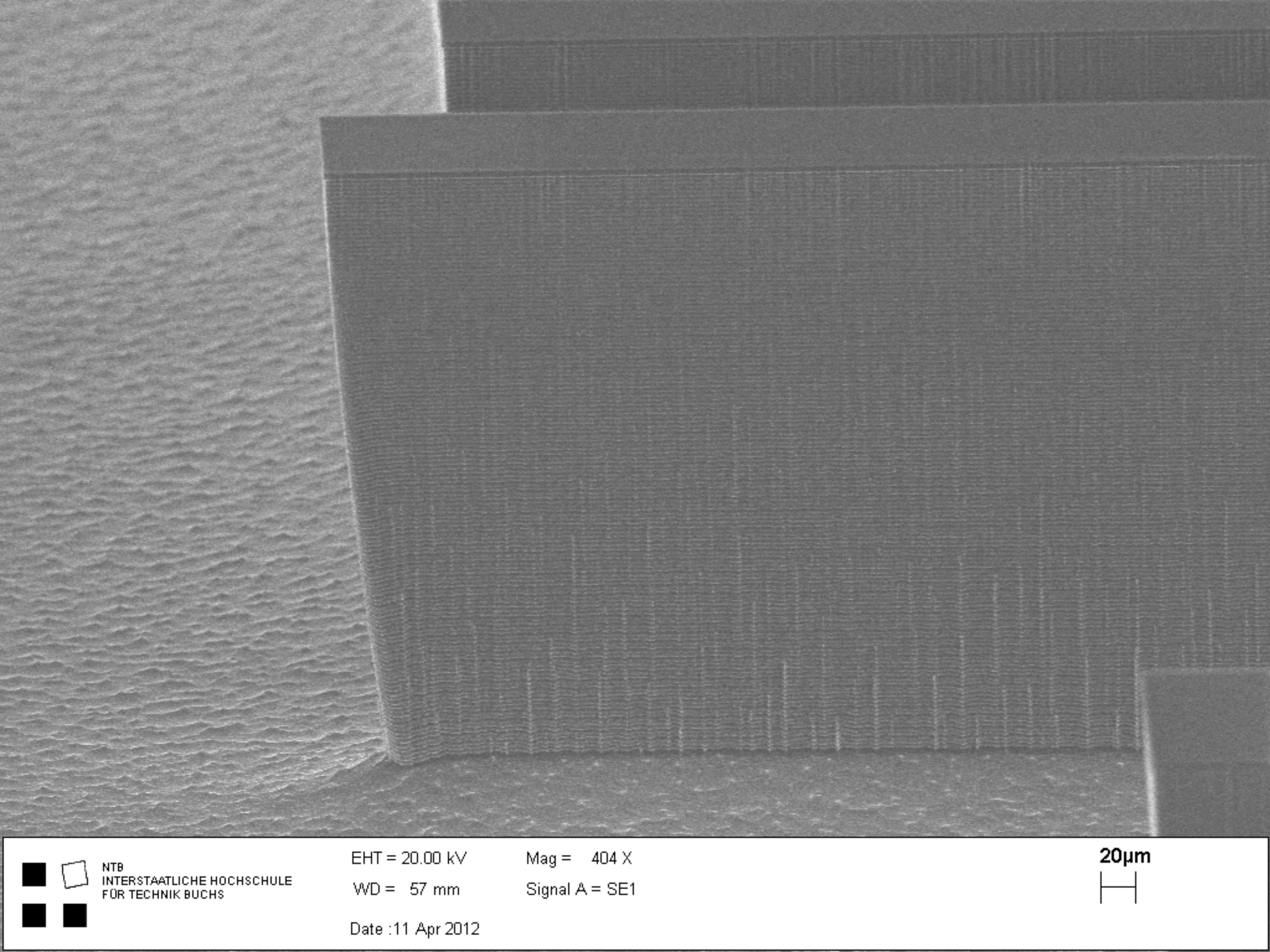
Fast silicon etch process with slightly opening profile. Suitable for deep etchings.
Fast Si Etch 2
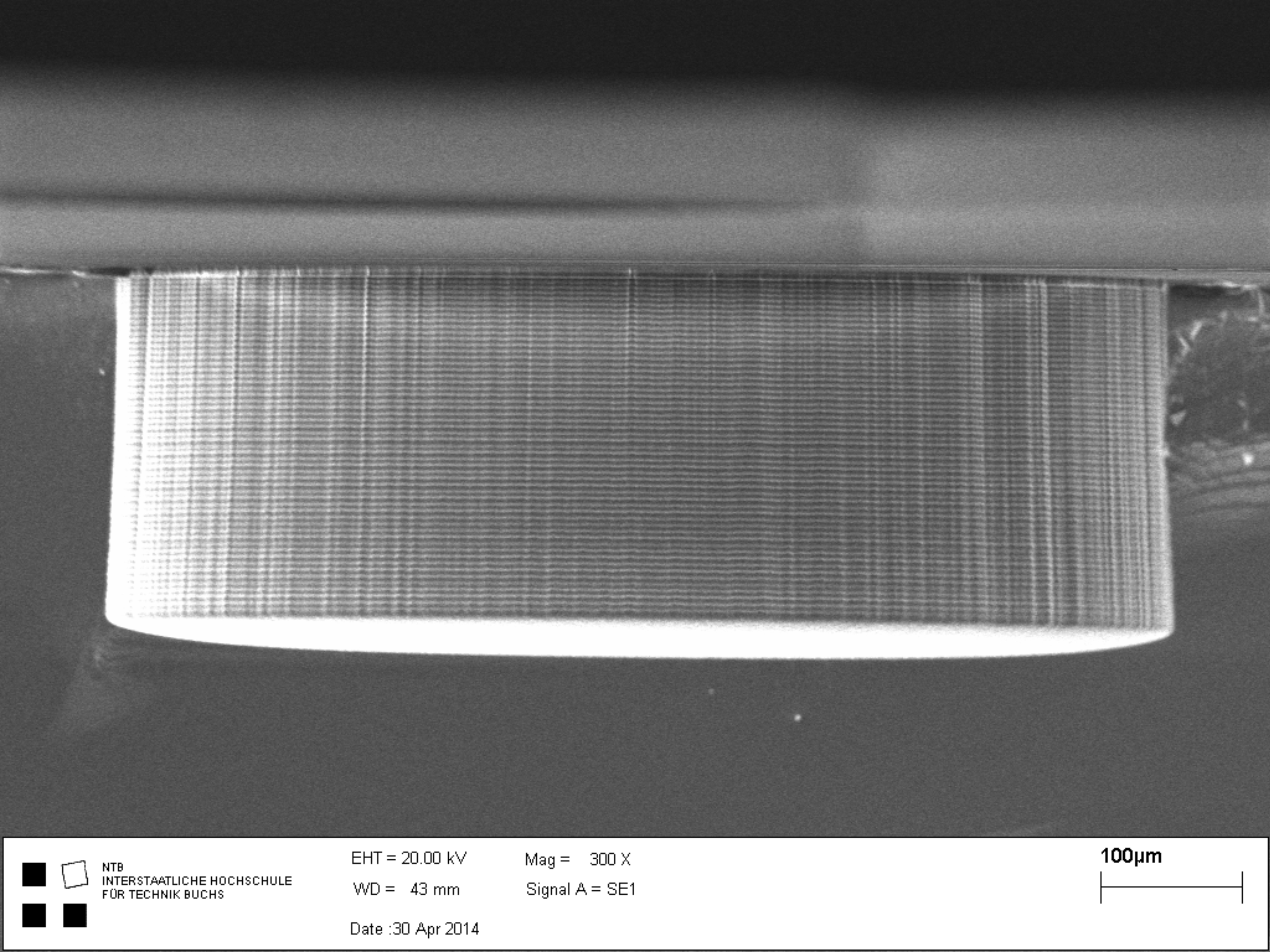
Fast silicon etch process, alternative to Fast Si Etch 1, suitable for deep etchings.
Slow Si Etch 90°

Silicon etch process with low etch rates but almost 90° side wall angle. Suitable for etchings of low depth (up to 100 μm) where vertical side walls are crucial. Also suitable for SOI-processes (Silicon On Insulator).
Amorphous Si Etch
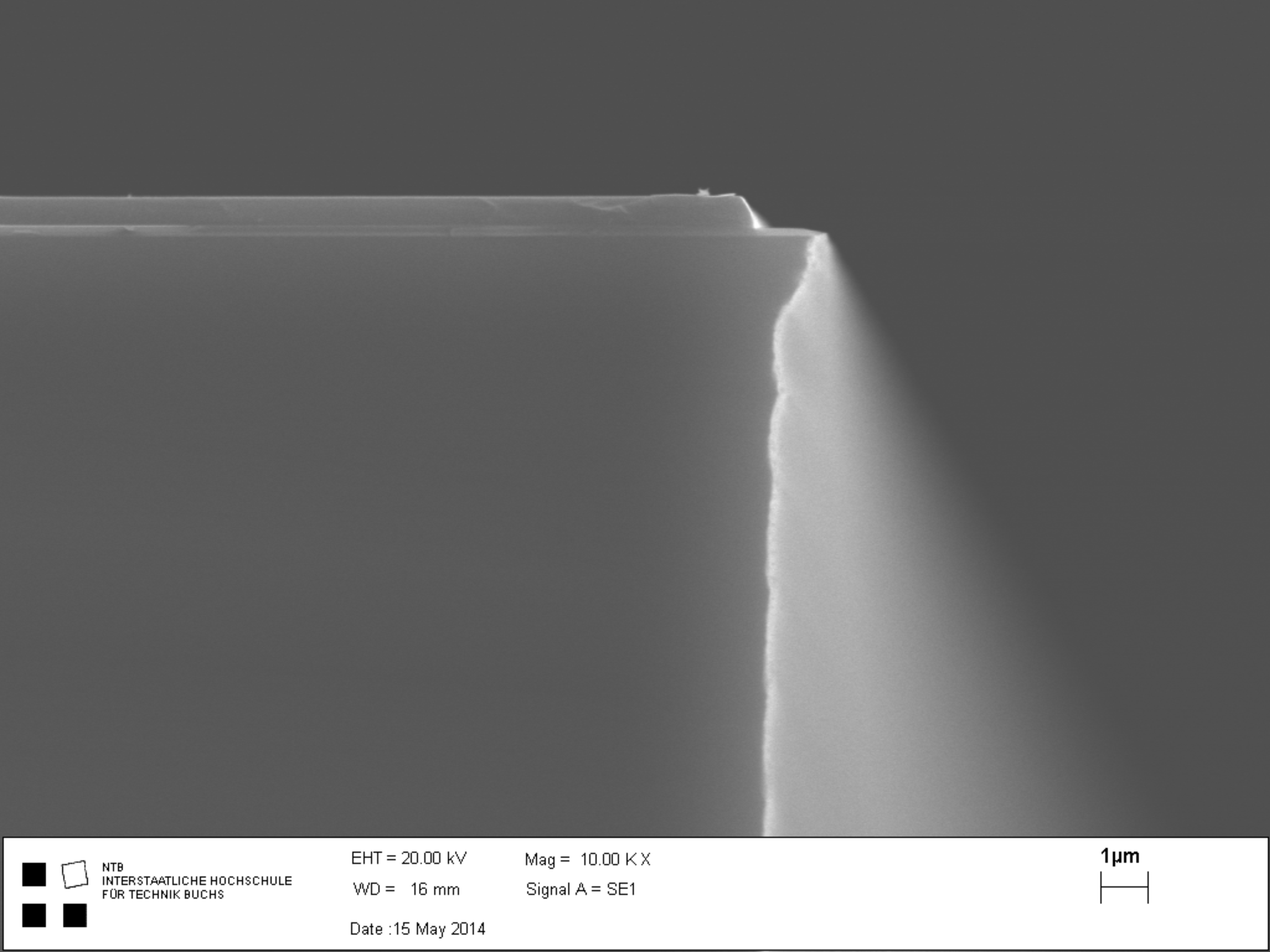
Patterning of amorphous silicon, suitable for thin films (up to 1 μm) of amorphous or polycrystalline silicon.
Prof. Dr. Martin Gutsche
IMP Institut für Mikrotechnik und Photonik Professor für Mikrotechnik, Leiter Kompetenzbereich Prozesstechnologie
+41 58 257 34 68 martin.gutsche@ost.ch


