Electron Microscopy
Scanning Electron Microscopy
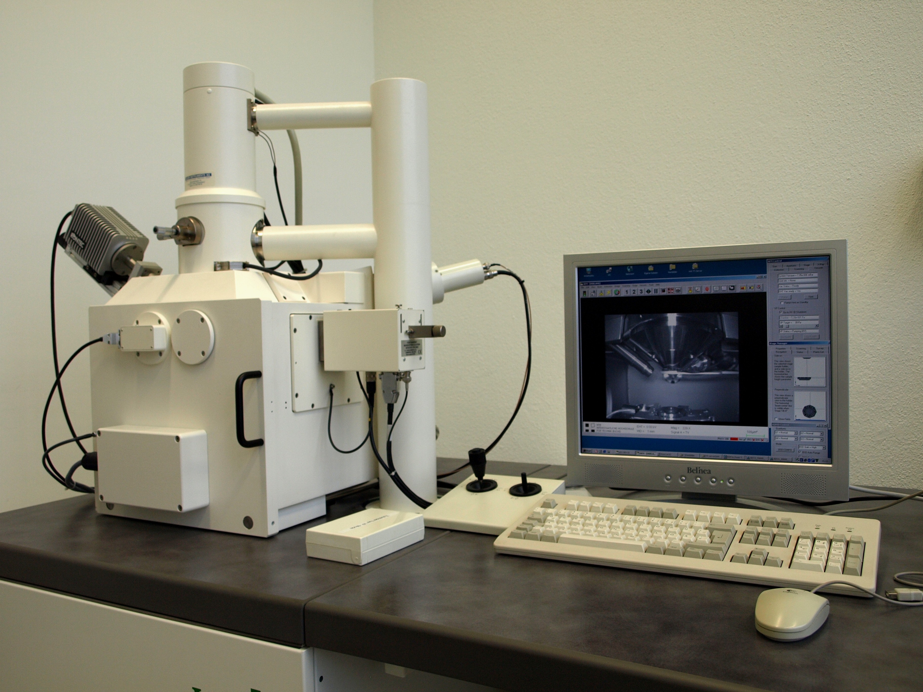
The miniaturisation of microelectronic components and the rapid development of new application fields such as nanoparticles necessitates the use of the Scanning Electron Microscope (SEM) to enable the characterisation of such products. The SEM allows magnifications that can visualize structures in the micro- and nanometer range. The possibility to either work in HV or under partial pressure and the various detectors enable the analysis of a wide field of materials. We characterize your surfaces and assess defects or identify the effects of altered process parameters in a fabrication process on the surface quality.

Energy Dispersive X-ray Fluorescence Analysis
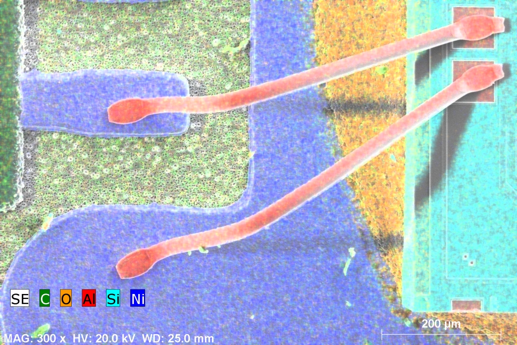
The SEM is extended by a energy dispersive x-ray fluorescence analysis (EDS) with which the chemical composition of a sample in the micrometer range can be identified. Different surface regions (spots, objects-mode) can be chosen to determine the phases of a microstructure, thus providing information about homogeneity, or to characterize defects. The line-scan-mode shows variations in electron concentration (e.g. at interfaces) and the element mapping mode visualizes the distribution of chemical elements on the surface.

Dietmar BertschIMP Institut für Mikrotechnik und PhotonikSenior Research Engineer, Fachverantwortlicher Packaging
+41 58 257 34 71dietmar.bertsch@ost.ch

