Thin Film Optics
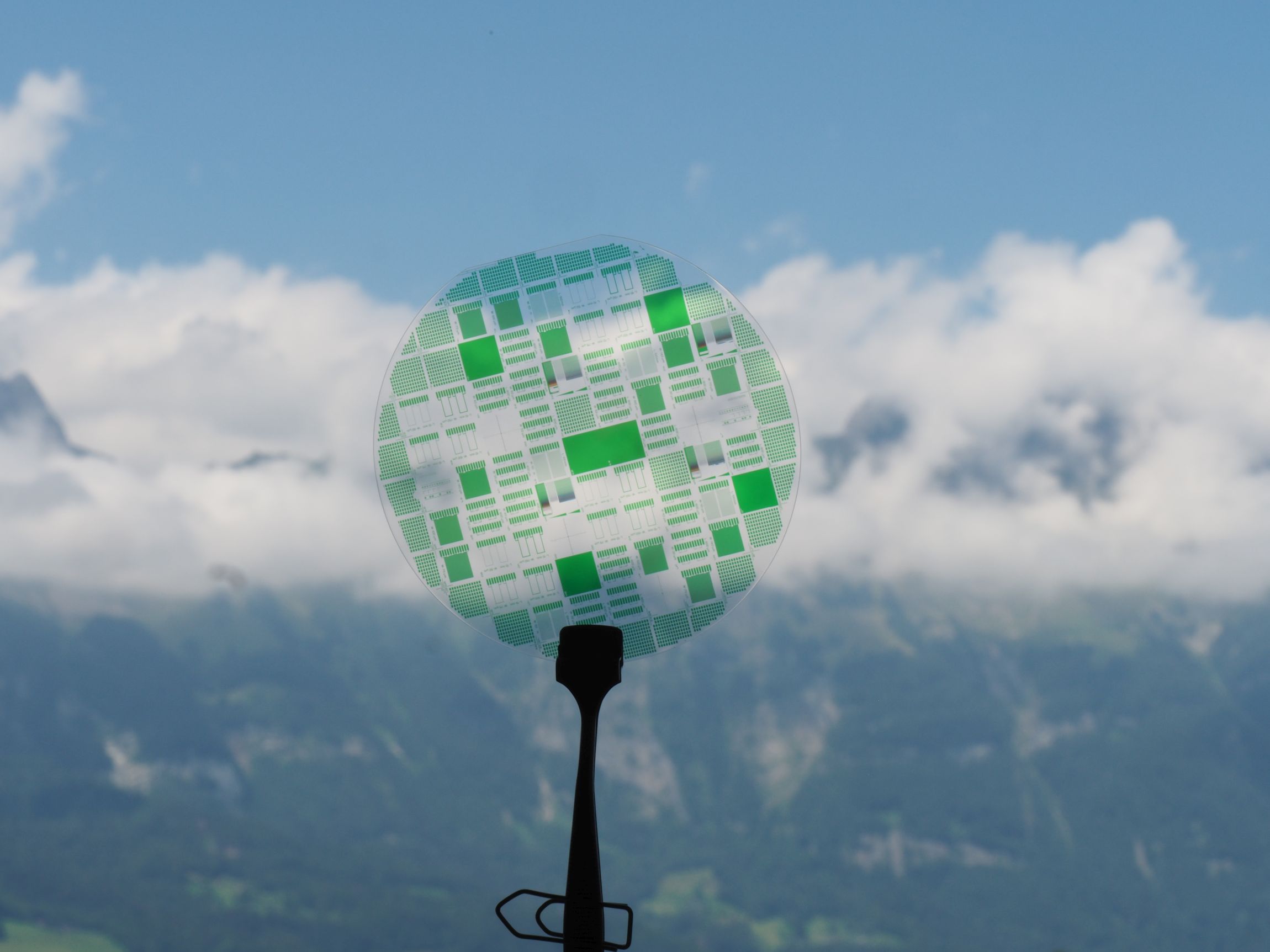
Dielectric thin film coatings of optical components and systems is a key to innovative and successful products.
Simulation of Thin Films
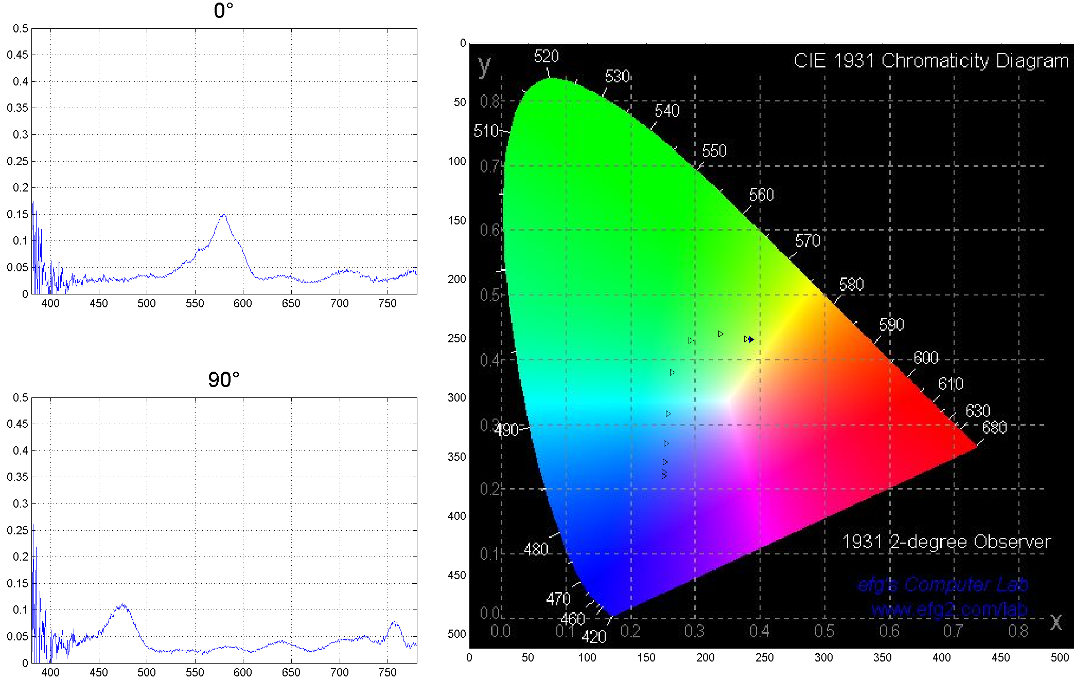
For the design and dimensioning of dielectric thin film coatings the calculation and modelling of reflective and transmissive properties of substrates and thin films are vital.
With the use of matrix-algorithms the spectral performance of various wavelengths and incident angles can be calculated. We solve such questions with the help of software packages like TFCalc and FilmStar, e.g. from simple layer calculations to optimization tasks or analysis of existing spectral curves.
Fabrication of Thin Films
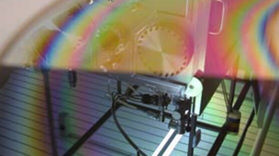
Within the scope of cooperation projects the MNT develops optical thin films or layer systems. Various methods, including coating processes like evaporation of single layers and simple anti-reflective or high-reflective coatings, are used. With our coating system from Evatec we can produce dielectric multi layer systems on small samples by ion-assisted sputtering.
Deposition Technologies
- PECVD - Deposition of silicon dioxide, silicon nitride und oxynitride at low temperatures
- PVD - Magnetron sputtering of silicon dioxide, titanium dioxide , niobium oxide und alumnium oxide
- PVD - Evaporation of silicon dioxide
- IBS - Ion beam sputtering of laser optics (in cooperation with Rhysearch)
- ALD - Atomic layer deposition of optical coatings (in cooperation with Rhysearch)
Thin Film Analytics
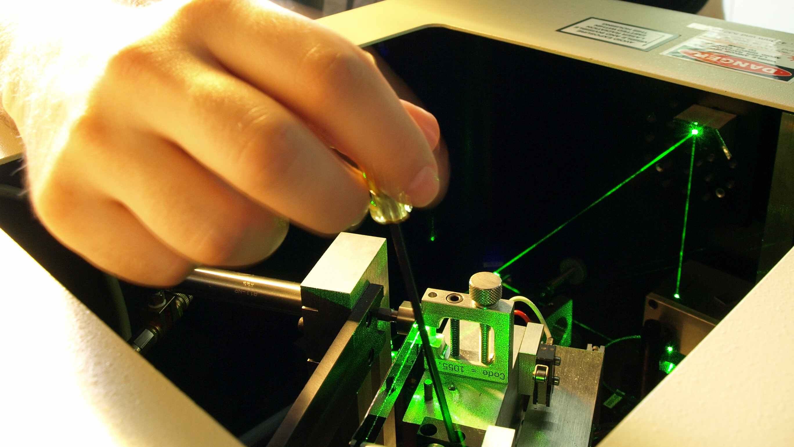
One of our core services we provide is the characterisation of optical thin films and layer systems. We determine the most important parameters of each layer including dispersion curves, spectral progression of refractive index, losses and thickness of your layer.
Furthermore we can determine the dispersion curve of your substrates as well as the spectral characteristics of your layer systems. For this task we use prism couplers by Metricon (m-line spectroscopy), reflection spectrometers, spectral photometers and optical spectrum analysers.
Measurement methods
- M-Line Spectroscopy
(thickness, refractive index, extinction) - Spectroscopy of Thin Films
(reflection, transmission) - X-Ray diffraction methods
(thickness, density, roughness) - Scanning Electron Microscopy with EDX
- Atomic Force Microscopy
- LIDT (in cooperation with Rhysearch)
- Measurement of optical losses in the ppm-range (Cavity-Ring-Down) (in coopeation with Rhysearch)
David Bischof
IMP Institut für Mikrotechnik und Photonik Projektleiter, Fachverantwortlicher 3D Laserbearbeitung von Glas
+41 58 257 34 91 david.bischof@ost.ch
Prof. Dr. Markus Michler
IMP Institut für Mikrotechnik und Photonik Professor für Physik und Photonik Leiter Kompetenzbereich integrierte Optik, Profilleiter Photonics
+41 58 257 34 64 markus.michler@ost.ch
